|
|
Backside illuminated photodiodes 2.9 - 5.5 µm (BSI PDs)
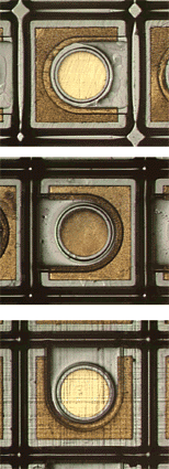
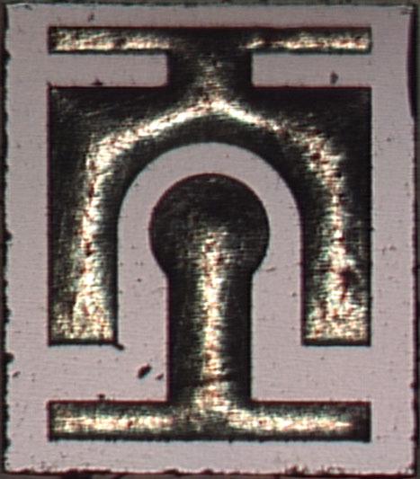
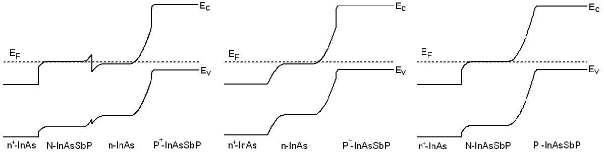
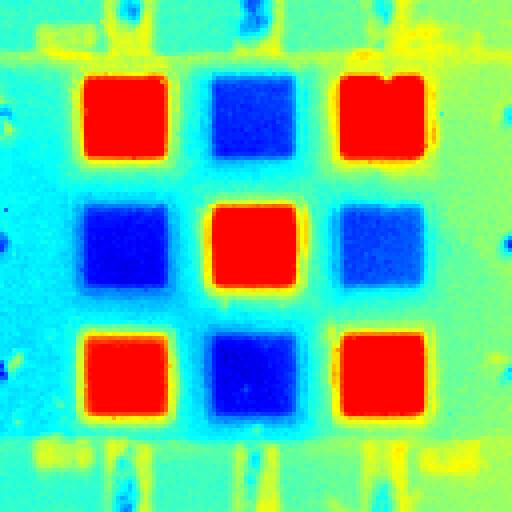
Fig.1 Photo (at the top) and schematic (at the bottom) of the LED/PD for 3.4 μm based on double heterostructure. Areas outside central mesa (near cathodes) are not active. The term "backside" means that photons pass through thick transparent (optically passive) substrate or thick buffer before they reach active zone with p-n junction (see Fig.1). Contrary to this in the front surface illuminated devices (FSI) the front (illuminated) surface is usually active and influences device performance. There has been an increased interest in ambient operating mid-infrared (λ =3-5 μm) light sources and detectors with respect to application in new spectroscopic analyzers. Optical components in this wavelength range are of particular interest for environmental monitoring, since most industrial gases have characteristic absorption bands in the above spectral range. For a number of years PbSe and pyroelectric based detectors have been commonly used for mid-IR (3-5 μm) sensing since they possess acceptable sensitivity to incandescent lamp output modulated by rotating chopper wheel. Recent progress in the design of fast and small λ =3.3 μm III-V LEDs with electrical or optical pumping initiated the need for fast detectors that are able to operate in a couple with a LED. It is a desire of an optical engineer to possess a diode with the possibility to couple it with the immersion lens or fibre and thus to obtain high signal to noise ratio or/and collimated beam. The “backside illuminated” (BSI) diode meets the above requirements since it does not contain any electrical contacts on the flat outer (or “window”) surface. However, commonly used InAs substrate absorbs radiation of interest and therefore there have been no practical realizations of the BSI constructions sensitive to 3.3 μm radiation. The BSI photodiodes are known for the narrow band InAsSb devices grown onto InAs transparent for the light at λ >4 μm. We present construction and characterization of the backside illuminated In(Ga)As(Sb) based photodiodes designed for several wavelengths utilizing heavily doped n+-InAs substrates, InAsSb(P) gradient transparent window or GaSb substrate. The diodes can be coupled with immersion lenses including hyperhemispherical ones. and may have up to 9 individually addressable elements (see Fig.2)
Fig 2. IR image of a 3x3 PD array with 4 elements emitting negative luminescence (NL, blue color) and 5 elements emitting electroluminescence (or "positive" luminescence -PL - red color)
|
|
|