|
|
FSI PD series
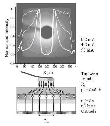
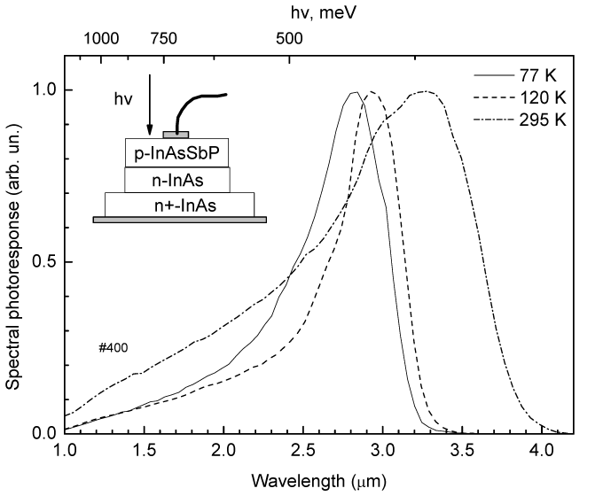
Fig.1 IR image (2.9 μm), radiation distribution along the diode (at the top) and equivalent electrical schematic of the InAs FSI PD(at the bottom). InAs photodiodes with InAsSbP transparent window layer, operating in the wavelength range 1.0-4.0 µm are based on InAsSbP/InAs system that is lattice matched and hence have low defect density and high performance. Heterostructures are grown on a ~350 µm thick n-InAs substrates (n=2*1016cm-3) and processed by a wet photolithography into circular or square mesa constructions. Fig.1 shows IR image and schematic of a square InAs PD. The quaternary layer InAsSbP acts as a window because the larger bandgap material is transparent to 3 µm radiation and thus most of the light is absorbed in the active region of the device. The composition and thickness of the widegap layer determines the short-wavelength cut-off value and the active region composition establishes the long-wavelength cut-off value of spectral response (see Fig.2).
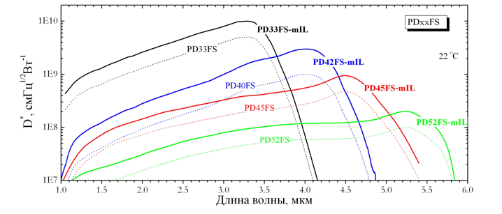
Fig.2 Spectral response of several FSI PDs at room temperature (horizontal scale in μm) The advantage of this structure is weak dependence of the quantum efficiency on the distance of the junction from the illuminated surface. Another advantage is that the heterostructure offers a reduced dark current because the wide bandgap layer usually has a lower equilibrium concentration of minority carriers which contribute to dark current. In contrast to flip-chip PDs, front surface illuminated PDs (FSI PDs) based on InAsSb with a limited area contact on the epitaxial side (see Fig.1) possess a broad photosensitivity spectrum, as they have no “built-in optical filter”, with a temperature-dependent absorption spectrum. A characteristic feature of diodes with a limited area contact is current crowding near the contact because of the predominance of the lateral resistance of the layer adjacent to the contact over the vertical resistance of the p–n junction at those regions of the diode which are distant from the contact, when the potential barrier at the p–n junction is low.
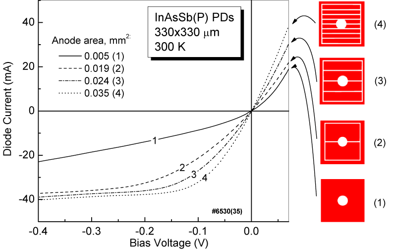
Fig.3 I-V characteristics of four 5.5 μm PDs with different anodes (1, 2, 3, 4) at room temperature. It was shown that InAsSb photodiodes (PDs) for the mid-IR spectral range (wavelengths λ > 4 μm) exhibit poor efficiency of photogenerated carrier collection from p–n junction regions distant from the anode at 25oC, which decreases by nearly an order of magnitude as temperature is elevated to 80oC, because of reverse current crowding. An increase in the anode perimeter makes it possible to raise, by an order of magnitude, the efficiency of nonequilibrium carrier collection and the sensitivity of InAsSb PDs at 25– 80oC. The dependence of the PD detectivity on the anode perimeter has a maximum. This occurs because, on the one hand, the area from which nonequilibrium carriers are collected becomes larger and, on the other hand, the degree of shading of the active region by the anode increases and the dynamic resistance of the PD decreases. On passing from a point anode to a developed anode, the current sensitivity and detectivity of the PD at 22oC become higher by a factor of 2 and 1.5, respectively . PDs effectively operating in the spectral range 2.2–4.5 μm were developed (see Fig.3, [1] ) . These diodes will be useful for solving a number of practical problems, e.g., in analyses of the content of CO2 in air. The fundamental aspects mentioned above are common to narrow-gap p–n structures ( see ref. [2], [3], [4]) and should be taken into account in the analysis of characteristics and the design of PDs, especially those operating at elevated temperatures in the photocurrent measurement mode.
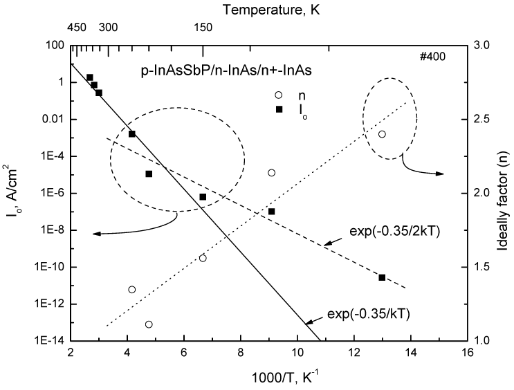
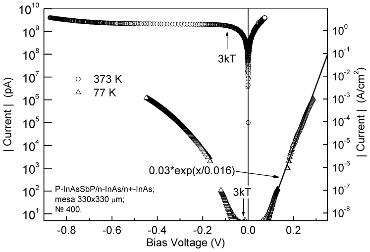
Cooling PD leads to sufficient performance enhancement, e.g. at 77 K InAs diodes exhibit excellent parameters as shown in figures below with D*λ value as high as 2.3 1013 cm Hz1/2W-1 [ 5 ] .
References
[1] N. D. Il’inskaya, A. L. Zakgeim, S. A. Karandashev, B. A. Matveev, V. I. Ratushnyi, M. A. Remennyi, A. Yu. Rybal’chenko, N. M. Stus’, and A. E. Chernyakov, Front Surface Illuminated InAsSb Photodiodes (Long_Wavelength Cutoff λ0.1 = 4.5 μm) Operating at Temperatures of 25–80°C, Semiconductors, 2012, Vol. 46, No. 5, pp. 690–695, Original Russian Text © N.D. Il’inskaya, A.L. Zakgeim, S.A. Karandashev, B.A. Matveev, V.I. Ratushnyi, M.A. Remennyi, A.Yu. Rybal’chenko, N.M. Stus’, A.E. Chernyakov, 2012, published in Fizika i Tekhnika Poluprovodnikov, 2012, Vol. 46, No. 5, pp. 708–713. [2] N. V. Zotova, S. A. Karandashev, B. A. Matveev, M. A. Remennyy, A. Yu. Rybal’chenko, and N. M. Stus’, ”Spatial nonuniformity of current flow and its consideration in determination of characteristics of surface illuminated InAsSbP/InAs-based photodiodes”, Semiconductors, 2011, Vol. 45, No. 4, pp. 543–549. © Pleiades Publishing, Ltd., 2011. ISSN 1063_7826, DOI 10.1134/S1063782611040245 Original Russian Text © N.V. Zotova, S.A. Karandashev, B.A. Matveev, M.A. Remennyy, A.Yu. Rybal’chenko, N.M. Stus’, 2011, published in Fizika i Tekhnika Poluprovodnikov, 2011, Vol. 45, No. 4, pp. 554–559. [3] S. A. Karandashev, B. A. Matveev, I. V. Mzhelskii, V. G. Polovinkin, M. A. Remennyi, A. Yu. Rybal’chenko and N. M. Stus’, “Nonuniformity in the spatial distribution of negative luminescence in InAsSb(P) photodiodes (long-wavelength cutoff λ0.1 = 5.2 μm)”, Semiconductors, Volume 46, Number 2, 247-250, DOI: 10.1134/S1063782612020157 . Original Russian Text © S.A. Karandashev, B.A. Matveev, I.V. Mzhelskii, V.G. Polovinkin, M.A. Remennyi, A.Yu. Rybal’chenko, N.M. Stus’, 2012, published in Fizika i Tekhnika Poluprovodnikov, 2012, Vol. 46, No. 2, pp. 258–261.
[4] N. D. Il’inskaya, S. A. Karandashev, B. A. Matveev, M. A. Remennyi, and N. M. Stus’, “Uncooled Photodiodes Based on InAsSb(P) with Long-Wavelength Sensitivity Boundary at λ = 5.8 μm”, ISSN 1063_7850, Technical Physics Letters, 2012, Vol. 38, No. 3, pp. 242–244..Original Russian Pis’ma v Zhurnal Tekhnicheskoi Fiziki, 2012, Vol. 38, No. 5, pp. 85–90. (DOI) 10.1134/S1063785012030078
[5] N. D. Il’inskaya, S. A. Karandashev, N. M. Latnikova, A. A. Lavrov, B. A. Matveev, A. S. Petrov, M. A. Remennyi, E. N. Sevost’yanov, and N. M. Stus’, “Cooled Photodiodes Based on a Type-II Single p-InAsSbP/n-InAs Heterostructure “ISSN 1063_7850, Technical Physics Letters, 2013, Vol. 39, No. 9, pp. 818–821. © Pleiades Publishing, Ltd., 2013. Original Russian Text © N.D. Il’inskaya, S.A. Karandashev, N.M. Latnikova, A.A. Lavrov, B.A. Matveev, A.S. Petrov, M.A. Remennyi, E.N. Sevost’yanov, N.M. Stus’, 2013, published in Pis’ma v Zhurnal Tekhnicheskoi Fiziki, 2013, Vol. 39, No. 18, pp. 45–52.
| |||||
|
|
 *
*