Generation and recombination of
carriers in p- and n-sides of a p-n junction govern a reverse current in the LEDs.
That’s why one can expect that electrons and holes may be efficiently extracted from p-n
junction vicinity with subsequent concentration fall well below equilibrium values. The
extraction means that n*p<no po=ni2
where n, p, and no, po refer to non-equilibrium and equilibrium
concentrations respectively and ni is the intrinsic concentration. This results
in the net absorption of ambient blackbody (BB) radiation, that is, the material can
absorb more radiation than it emits which is equivalent to lower effective device
temperature. Thus, the reverse biased (RB) device work as a “light absorbing diode”
(LAD) with corresponding phenomena known as a “negative luminescence” (NL).
NL intensity grows on both wavelength and temperature (T)
increase which reflects the BB radiation properties. However, this is not the
case for the FB LEDs because Auger recombination strongly enhances with energy band gap
and (1/T) decrease. There is, thus, a “crossover temperature” which indicates the
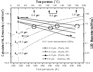
starting point of superiority of NL efficiency over that of FB LEDs. Fig.1 presents
experimental and simulated data relative to determination of the “crossover
temperature” in the 20-180oC range: best room temperature (RT) LED outputs
taken from literature and expectations of LED power at high temperatures obtained through
the experimental power quenching coefficient. There is a lot of enthusiasm for NL devices
with wavelengths longer than 4 mm since the “crossover
temperature” is only 60 and 100-120oC for 6 and
4.3 mm LEDs correspondingly. So, NL LED operation at elevated
temperatures can thus bring more benefits than conventional forward bias (FB) operation
mode.
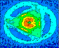
Fig.2 presents FB triangle diode image recorded by
CdHgTe (77 K) (l
=3-5
mm) based thermal camera at 55oC (by
Prof.Malyutenko V.K., Kiev). The image reflects the
drop of a signal at the contact (green area at the triangular center) and the signal
decreasing from center to edge (in FB mode) i.e. an evidence for current crowding.
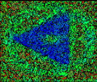
In contrast to Fig.2 the negative luminescence
image (Fig.3) “inherits” some of the positive luminescence
peculiarities: small signal at the contact. However, the apparent
temperature distribution is nearly uniform. That is because of the increase
of resistance of a p-n junction in a reverse bias.
Additional information on negative luminescence devices can be found in
publications.
including overviews by
Malyutenko (1995)
and
Ivanov-Omskii
(2007).