|
1 |
U>0 |
p-GaSb LED with nonuniform
radiation pattern
(0.5x0.5 mm).
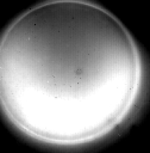
Semiconductors, 2009, Vol. 43, No. 5, pp. 662–667
|
InAs PD with point contact at
forward bias
(0.5x0.5 mm).
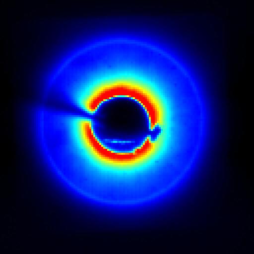
Semiconductors, 2011, Vol. 45, No. 4, pp. 543–549 |
|
|
2 |
U=0 |
InGaAsSb LED array with external
lightning
(0.5x0.5 mm).
Proc. of SPIE Vol. 7223 72231B-1 |
InGaAsSb LED array at thermodynamic
balance
(0.5x0.5 mm)
Proc. of SPIE Vol. 7223 72231B-1 |
|
|
3 |
U>0 |
InGaAsSb 1x4 LED array with photonics
crystal structure (all 4 elements are biased)(2x2 mm) .
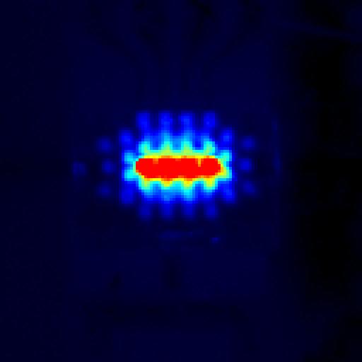
Proc. of SPIE Vol. 7609, 76090I-1
-5 |
InGaAsSb 1x4 LED array with photonics
crystal structure (only 2 elements are biased)(2x2 mm).
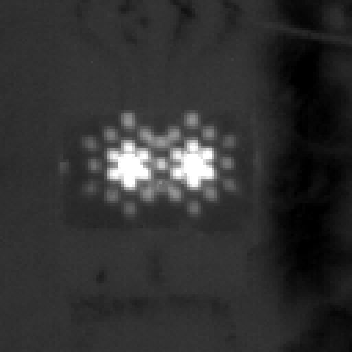
Proc. of SPIE Vol. 7609, 76090I-1
-5 |
|
|
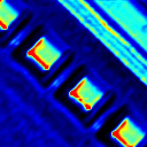
4 |
U> 0
U<0 |
InGaAsSb 1x4 LED array with reverse (left) and forward
(right) biasing of elements (0.5x0.5 mm).
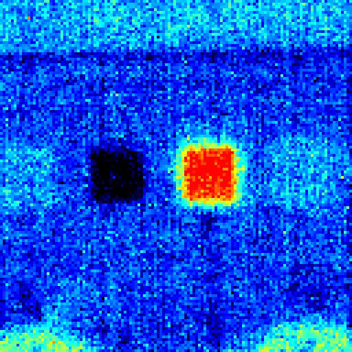
Proc. of SPIE Vol. 7223 72231B-1 |
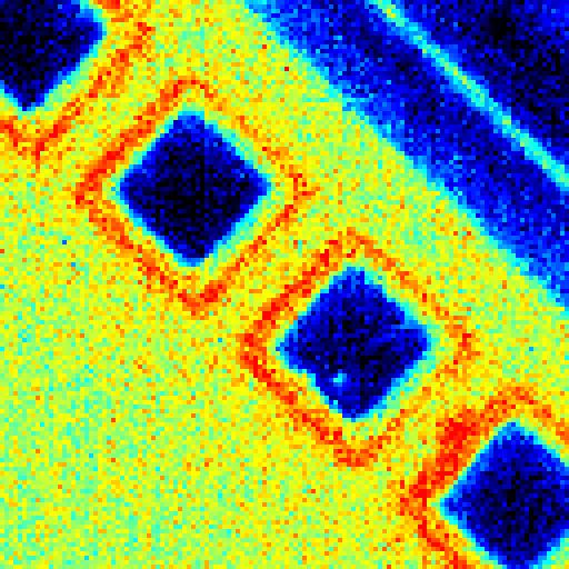
InAs 3x3 LED array with 4 elements at reverse bias and
5 -- at forward bias (2x2 mm).
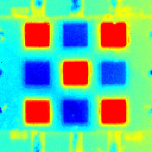
www.ioffeled.com |
|