|
| |
Surface illuminated InAs photodiodes
3.0-3.3 mm
|
|
Basic parameters
at t=20 0C
|
PD Type |
Wavelength,
µm |
Spectrum FWHM,
µm |
Sensitive
area, mm |
Visual angle
deg. |
Ro,
W |
SU l
max,
V/W |
SI l
max,
A/W |
D*l
max,
cm Hz1/2W-1 |
|
SE |
3.0 |
³1 |
0.43 |
140 |
³0.25 k |
³250 |
³1 |
~5´109 |
|
micro IL |
1.0 |
<30 |
~7.5´109 |
|
- InAs photodiodes
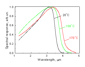
with InAsSbP transparent window layer, operating in the wavelength range 1.0-4.0 µm are
based on InAsSbP/InAs and systems that is lattice matched and hence low defect density and
high performance are expected. Heterostructures were grown by the LPE method on a 350 µm
thick n-InAs substrates (n=2*1016cm-3) and processed by a wet
photolithography into a mesa constructions.
- The quaternary layer InAsSbP acts
as a window because the larger bandgap material is transparent to 3 µm radiation and thus
most of the light is absorbed in the active region of the device. The composition of the
widegap layer determines the short-wavelength cut-off value and the active region
composition establishes the long-wavelength cut-off value of spectral response. One
advantage of this structure is the relative independence of the quantum efficiency on the
distance of the junction from the illuminated surface. Another advantage is that the
heterostructure can offer a reduced dark current because the wider bandgap layer usually
has a lower equilibrium concentration of minority carriers which contribute to the
diffusion current.
|
|
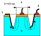
p-InAsSbP/n-InAs
photodiode section view. 1- InAsSbP window layer, 2-InAs substrate,
3-cathode, 4-anode
 |
|