|
| |
- InAs(Sb) LEDs and negative luminescent devices for
dynamic scene simulation in the first atmospheric window (3-5
mm)
-
Volodymyr Malyutenko, Oleg Malyutenko,
Andrey Zinovchuk
-
Institute of Semiconductor Physics,
Kiev, Ukraine, FAX: (044) 265
57 97, e-mail:
malyut@isp.kiev.ua
- Nonna Zotova,
Sergey Karandashev, Boris Matveev, Maxim Remennyi, Nicolay Stus
- Key words:
3 to 5 microns range, LEDs, IR scene simulation.
-
- We
report on the test results of 3 to 5 um wavelength light-emitting diodes
(LEDs), which simulate highest apparent temperature (Ta) values for
photonic emitters yet, reported. Points of our concern are maximum power
emitted in both positive and negative modes, uniformity of light pattern in
micro scale (current crowding effect), and possible effect of a structure base
overheating on a device performance.
-
The 3.3-3.4
mm
LEDs were grown as lattice matched InAsSbP/InAs double heterostructures
(DHs) by the LPE process onto heavy doped and therefore
practically transparent for emitting
wavelength InAs substrate.
The
DH consisted of 1-1.5
µm thick wide-gap n-InAs1-x-ySbxPy (0.08<x<0.09,
0.15<y<0.19) confining layer, 0.5-1
µm thick n-InAs active region and 2-3µm thick wide-gap p-InAs1-x-ySbxPy(Zn)
(0.08<x<0.09,
0.15<y<0.19)
emitter. The n-InAs active region was grown from the melt with gadolinium
ions as a gettering agent; this type melt purification process reduces the
concentration of non-radiative recombination centers and therefore increases
quantum efficiency of the structure.
The epilayers for the 4-4.7
mm
LEDs
have been grown as 25¸60
mm
thick InAsSbP graded band gap structures. The layers were characterized by
low dislocation density (104 cm-2) due to lattice
match conditions at heterojunction and smooth increase of lattice parameter
to the surface which make possible “inverse defect formation”. The samples
were curved with R=10¸15
cm and were characterized by an increase of antimony and the decrease of
phosphorus concentrations towards the epilayer surface
-
The
wafers were processed by a wet photolithography into circular (D=300 µm)
mesa chips. Ohmic contacts (central circular anode of d=150 µm and
peripheral 'U-shaped' cathode) were formed by thermal
evaporation of Au. Both chip contacts were soldered to contact area of a
1.5x1.7x0.4 mm3 semi insulating Si submount. Next, the Si
submounts with LED chip were soldered onto a TO-39 header in substrate up
manner. Some LEDs were equipped with immersion lens made from CdSb and
attached to the LED surface by a chalcogenide glass. The full width at
half-maximum of the collimated beam escaping the structure through substrate
and lens was less then 250.
-
The IR micro mapping system we developed consists of reflective-type IR
microscope co-axially attached to scanning IR thermal imaging camera
operated in the 3-5
mm
spectral range with HgCdTe cooled photo detector. This system permits scene
spatial resolution better than 20
mm,
the 10
ms
minimum time-resolved interval, and temperature resolution of about 0.10C.
In addition, the system is capable of operating in external triggering mode
with noise reduction by image averaging1.
-
 Operating
in extreme modes (50 usec pulse duration, 25 Hz repetition rate, I=1 A) and
recorded by 3 to 5 mm
infrared microscope, the devices are capable of simulating dynamic apparent
temperature ΔT = 300 K at room temperature and ΔT
³ 500
K when cooled down to T=200 K (positive contrast devices). We show that
the results achieved are due to charge carrier confinement, intended structure
doping by rare-earth metals, improved heat sink and internal beam focusing in
a transparent substrate-up mesa structure. We show also that the most
effective room temperature negative contrast devices are 4.4
mm-emitting
structures. By comparing these LEDs to the conventional edge-emitting diode
lasers, we show that conventional non-resonant IR LEDs are becoming an
important candidate to form the basis for IR (3 to 5
mm)
dynamic scene simulation devices. Operating
in extreme modes (50 usec pulse duration, 25 Hz repetition rate, I=1 A) and
recorded by 3 to 5 mm
infrared microscope, the devices are capable of simulating dynamic apparent
temperature ΔT = 300 K at room temperature and ΔT
³ 500
K when cooled down to T=200 K (positive contrast devices). We show that
the results achieved are due to charge carrier confinement, intended structure
doping by rare-earth metals, improved heat sink and internal beam focusing in
a transparent substrate-up mesa structure. We show also that the most
effective room temperature negative contrast devices are 4.4
mm-emitting
structures. By comparing these LEDs to the conventional edge-emitting diode
lasers, we show that conventional non-resonant IR LEDs are becoming an
important candidate to form the basis for IR (3 to 5
mm)
dynamic scene simulation devices.
-
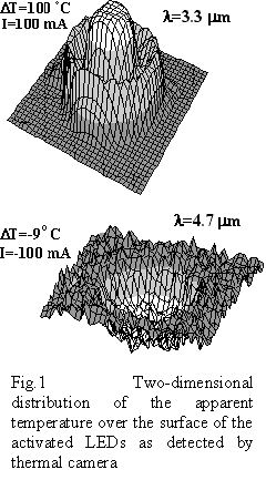
Shown in Fig.1
are some results of high-resolution mapping (28 ms frame duration) of
radiation emitted by InAs (l=3.3
mm,
top) and InAsSb (l=4.7
mm,
bottom) mesa down LEDs. Being spatially uniform at low forward bias the light
spatial distribution suffer of current crowding, that results in concentration
of light over central
circular contact
(conventional electroluminescence mode). That is not the case for reverse bias
mode (negative luminescence) 2,3.
-
The work of the was partly supported by the Ministry of
Education and Science of Ukraine and EOARD contract (Ukrainian team) and by
the SBIR/STTR program (Russian team)
-
-
1.
V. Malyutenko, Proc. SPIE, 5092, 83-86, 2003 .
- 2. V.K.
Malyutenko, O.Yu. Malyutenko, A.D. Podoltsel, I.N. Kucheryavaya, B.A. Matveev,
M.A. Remennyi, and N.M. Stus, Appl. Phys.
Lett. v.79(25),
p. 4248-4250, 2001
3. V.К.
Malyutenko, 0.Yu. Malyutenko, A. Dazzi, N. Gross, J-M.
Ortega, J. Appl. Phys.
v.93(11), 9398-9400, 2003
|